

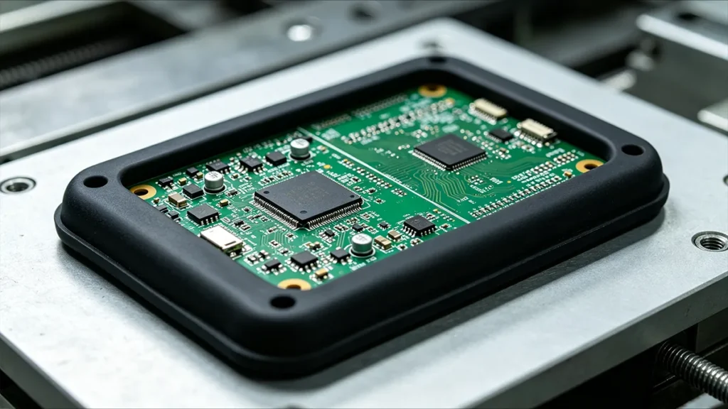
قد تبدو مجموعة مفاتيح عجلة القيادة جهازًا بسيطًا، لكنها معقدة في تصميمها. تتضمن المجموعة مصابيح LED ومقاومات ومكثفات ومفاتيح لمسية ولوحة دوائر مطبوعة من نوع FR-4 وموصلًا مخصصًا للسيارات ووحدة تحكم دقيقة. ويجب توفير الحماية الكافية لهذه الأجهزة أثناء تشغيل السيارة. تتعرض السيارة لبيئة قاسية تتميز بالرطوبة والاهتزازات والتقلبات في درجات الحرارة والأحمال الميكانيكية، مما يستلزم بشكل صارم الامتثال لمعايير الموثوقية البيئية مثل ISO 16750 الخاصة بالإلكترونيات الخاصة بالسيارات [1]. من الضروري اختيار عملية التصنيع المناسبة لحماية هذه الأجهزة في بيئة التشغيل هذه. وتُعدّ طريقة التصنيع المفضلة هي القولبة الفوقية للوحة الدوائر المطبوعة (PCB) باستخدام المطاط الحراري (TPE). وتتميز لوحة الدوائر المطبوعة المقولبة عزلًا كهربائيًا وحمايةً ضد الاهتزازات.
ما المقصود بـ«القولبة الفوقية للوحات الدوائر المطبوعة»؟
يُعرف «القولبة الفوقية للوحات الدوائر المطبوعة» (PCB) بأنها عملية تغليف لوحة دوائر مطبوعة مجمَّعة بالمطاط أو البلاستيك باستخدام تقنية القولبة بالحقن. حيث تُوضع مجموعة اللوحة الدائرة المطبوعة في قالب مصمم خصيصًا، ثم تُسكب المادة المنصهرة في التجويف. وبعد أن تبرد المادة، تتشكل قشرة واقية صلبة حول اللوحة.
عملية القولبة الفوقية للوحات الدوائر المطبوعة (PCB)
تشبه عملية القولبة الفوقية للوحات الدوائر المطبوعة (PCB) إلى حد كبير عملية القولبة بالحقن التقليدية. وفي الواقع، تستخدم هذه العملية معدات مشابهة لتلك المستخدمة في القولبة بالحقن التقليدية. ومع ذلك، فإن نطاق المعلمات المسموح بها في عملية القولبة الفوقية للوحات الدوائر المطبوعة (PCB) أضيق بكثير منه في حالة اللدائن العادية. وفيما يلي التسلسل الزمني لخطوات عملية القولبة الفوقية للوحات الدوائر المطبوعة (PCB):
- فحص لوحات الدوائر المطبوعة
- التنظيف / التجفيف
- إدراج
- التحميل والتثبيت
- إغلاق القالب
- الذوبان
- الحقن
- التعبئة / التخزين
- التبريد
- فتح القالب
- الطرد
- التشذيب + الفحص
- الاختبارات الكهربائية / الوظيفية
1. فحص الدائرة المطبوعة (PCB)
قبل البدء في عملية القولبة الفوقية، تأكد من أن جميع الدوائر على لوحة الدوائر الكهربائية قد تم لحامها بالكامل واختبارها للتأكد من عدم وجود أي مشكلات. وبمجرد اكتمال عملية التغليف، يصبح من المستحيل إعادة معالجة الأجزاء الداخلية. وبعد التأكد من كل شيء، تتمثل الخطوة التالية في تنظيف لوحة الدوائر الكهربائية. في بعض الأحيان، يلزم تطبيق طبقة أساس على السطح لتعزيز الالتصاق بين المادة ولوحة الدوائر الكهربائية ولمنع حدوث انفصال في المستقبل أو تسرب المياه.
2. تصميم القوالب وتصنيعها
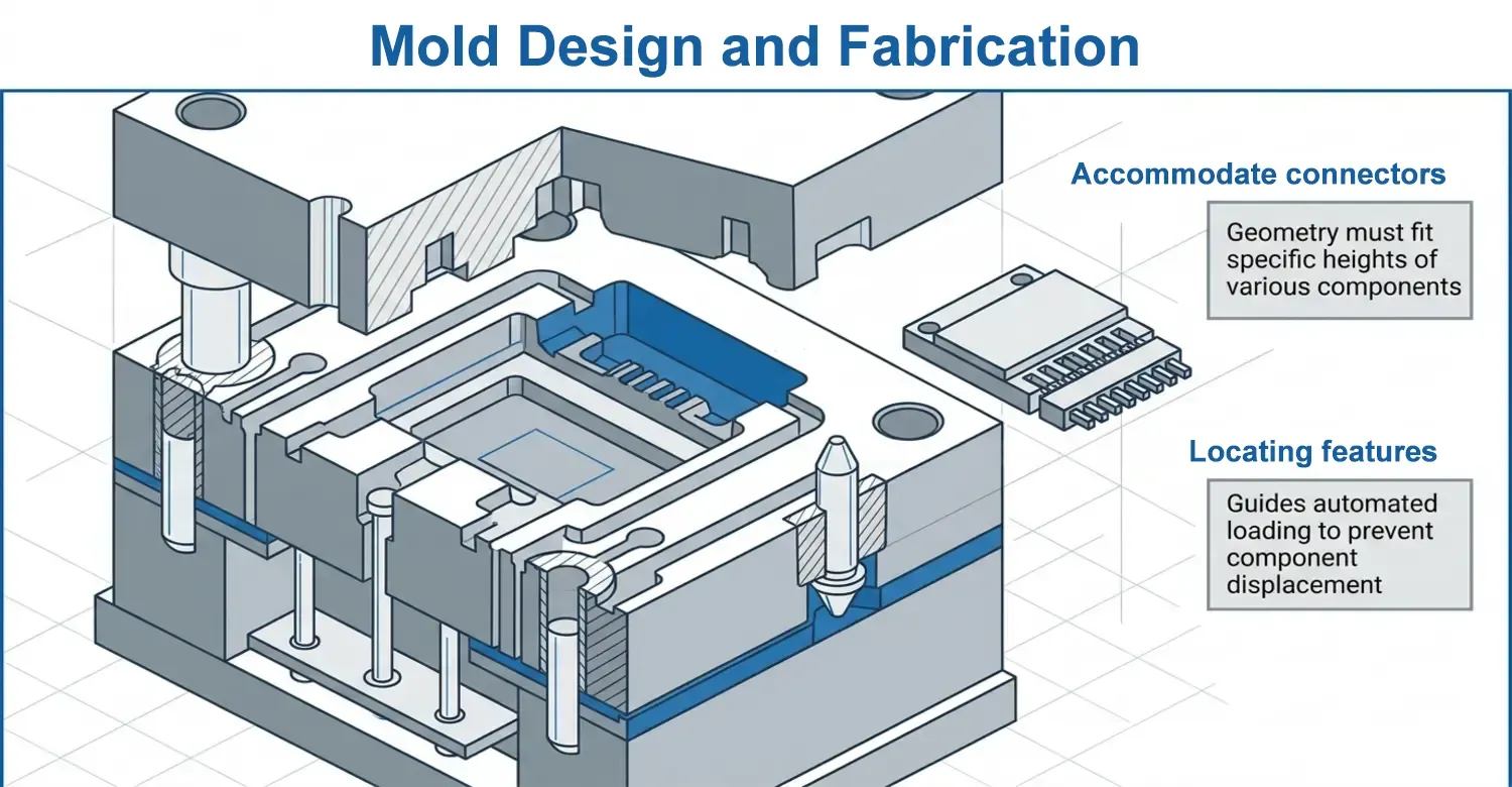
يتم تحقيق النجاح في عملية القولبة الفوقية للوحات الدوائر المطبوعة (PCB) من خلال الاستثمار في تصميم القالب. يتميز تجويف القالب المستخدم في عملية القولبة الفوقية للوحات الدوائر المطبوعة بهندسة تختلف عن تلك المستخدمة في القولبة بالحقن العادية. ويجب أن يستوعب التجويف الموصلات ووصلات اللحام والمكونات الإلكترونية. ويجب على المصمم التأكد من تثبيت القالب بشكل فعال لتجنب أي حركة أثناء عملية الحقن. فأي إزاحة صغيرة جدًّا غير مرغوب فيها لأنها قد تؤدي إلى اختلال محاذاة الموصلات، وتفاوت سماكة التغليف، وتلف المكونات. وإذا كان القالب مخصصًا لإنتاج كميات كبيرة، فمن الضروري استخدام ميزات تحديد الموضع لتوجيه عملية تحميل لوحات الدوائر المطبوعة آليًّا.
يجب إجراء فحص فعال للقالب قبل عملية القولبة. يساعد الفحص المسبق على تحديد التلوث المحتمل وعيوب اللحام. وبمجرد فحص القالب، يجب تنظيفه لمنع التصاق البوليمر وتشكل الفراغات، مما يؤثر على جودة المنتج. قد يشمل التحضير أيضًا تجفيف القالب، خاصةً عند استخدام البوليمرات الحساسة للرطوبة. يمكن لهذه البوليمرات امتصاص الماء، والذوبان، وتغيير خصائصها الكيميائية والفيزيائية عند تعرضها لبيئات رطبة. ومن أمثلة البوليمرات الهندسية الحساسة للرطوبة التي تُستخدم عادةً في عملية القولبة الفوقية: النايلون (البولي أميدات)، والبولي يوريثان (PU)، وبعض أنواع اللدائن الحرارية المرنة (TPE).
3. التحميل وإغلاق القالب
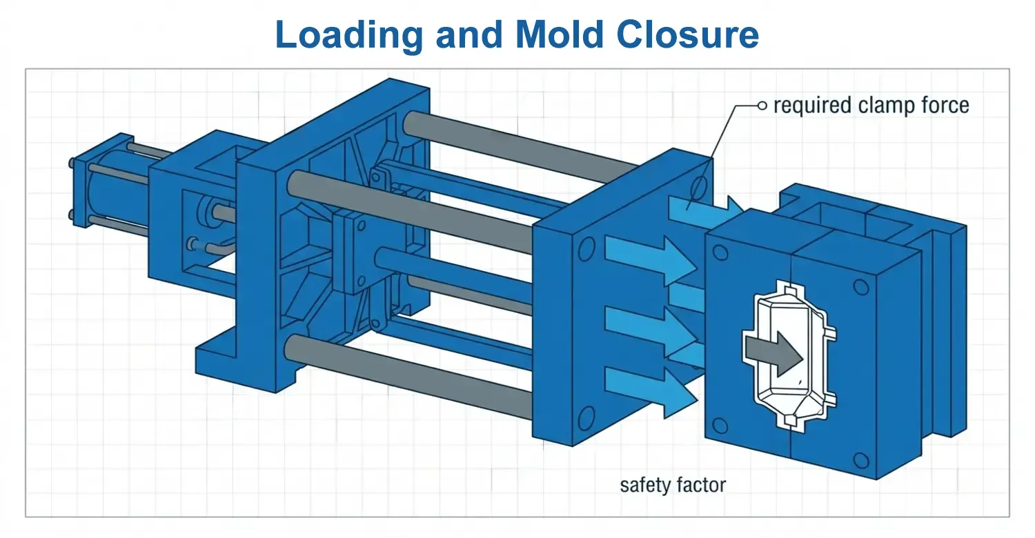
بعد الفحص، تُوضع لوحة الدوائر المطبوعة المُجمَّعة (PCBA) في القالب المصمم. ويحافظ القالب على موضعه بدقة لضمان تدفق المادة المُغلفة بدقة إلى كل منطقة دون الإضرار بالمكونات. وبمجرد اكتمال التحميل، يقوم المشغل بإغلاق القالب حول لوحة الدوائر المطبوعة (PCB) لبدء عملية الحقن. يتم حقن المادة المنصهرة في التجويف تحت الضغط، مما يعني تطبيق قوة تثبيت كافية. عند اختيار قوة التثبيت، تأكد من أنها أعلى من قوة التثبيت المطلوبة. وتُعبَّر عن هذه العلاقة بالصيغة التالية:;
Fc = PcApS
حيث Fc هي قوة التثبيت المطلوبة، وPc هو الضغط الفعال في التجويف، وAp هي المساحة المسقطة للمكون المصبوب. وS هو معامل الأمان. على سبيل المثال؛;
Pc=60 ميجا باسكال، و Ap= 0.004 م²، إذن
Fc=60×106×0.004=240 كيلو نيوتن.
عند تصميم القالب، اختار المهندسون معامل أمان لضمان أن تتجاوز قوة التثبيت ضغط التجويف. على سبيل المثال، يؤدي اختيار معامل أمان يبلغ 1.5 إلى ضبط قوة التثبيت عند 360 كيلو نيوتن، وهو ما يُعد أكثر أمانًا بكثير لحقن المواد المنصهرة. يجب اختيار قوة التثبيت بقيمة معتدلة. فقد تؤدي قوة التثبيت غير الكافية إلى ظهور نتوءات عند خط الفصل، في حين أن قوة التثبيت المفرطة قد تزيد من إجهاد القالب واستهلاك الطاقة.
4. صهر البلاستيك والحقن
يحتوي أسطوانة طويلة أسطوانية الشكل مزودة ببرغي دوار على عناصر تسخين تعمل على إذابة الراتينج البلاستيكي. ويقوم البرغي بخلط الراتينج وزيادة الضغط عليه، مما يدفعه إلى الأمام. يُحقن البلاستيك المنصهر في التجويف تحت ضغط مُحكَم. ويتفاوت الضغط بسبب عوامل مختلفة مثل السرعة، وسماكة الجدار، ولزوجة البوليمر، وتصميم فتحة الحقن، كما هو ملخص في معادلة التدفق النيوتوني عبر قناة دائرية المعطاة بالصيغة التالية:;
ΔP ≈ 8μLQ/(πR⁴) [2]
حيث يمثل ΔP انخفاض الضغط، وμ لزوجة المادة المنصهرة، وL طول التدفق، وQ معدل التدفق الحجمي، وR نصف قطر التدفق الفعال. ورغم أن معظم المواد البلاستيكية لا تتبع معادلة التدفق النيوتونية هذه، إلا أنها توجه المهندسين في تحديد المناطق الحرجة التي يجب مراقبة عند ممارسة ضغط الحقن أو تنظيمه.
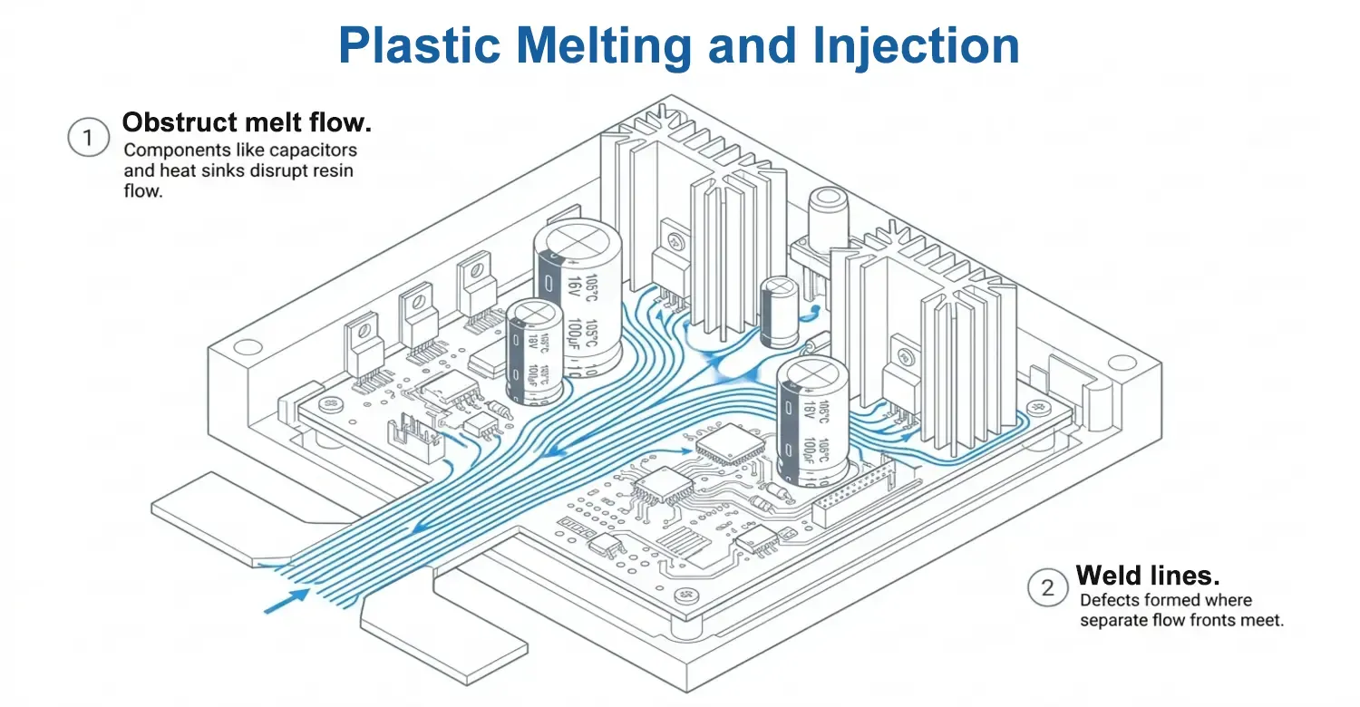
يُعد تدفق المواد داخل تجويف القالب في عملية القولبة الفوقية للوحات الدوائر المطبوعة (PCB) أكثر تعقيدًا مقارنةً بالقولبة بالحقن التقليدية. تحتوي مجموعة لوحات الدوائر المطبوعة (PCB) على حواف لوحات الدوائر المطبوعة، ومكثفات، ووصلات لحام، وحزم الدوائر المتكاملة (IC)، وموصلات، وأسلاك، ومبددات حرارية، ومكونات أخرى طويلة. يمكن أن تعيق هذه المواد تدفق المادة المنصهرة. وإذا لم يتم التعامل مع هذا العائق بشكل جيد، فقد يؤدي ذلك إلى ظهور خطوط لحام تضر بجودة المنتج.
5. التبريد والتصلب
بمجرد ملء التجويف، يجب إزالة الحرارة من البوليمر. ويتناسب معدل إزالة الحرارة تناسبًا مباشرًا مع سماكة الجدار.
tc ∝ s2
حيث tc هو وقت التبريد، و s هي سماكة البوليمر المميزة.
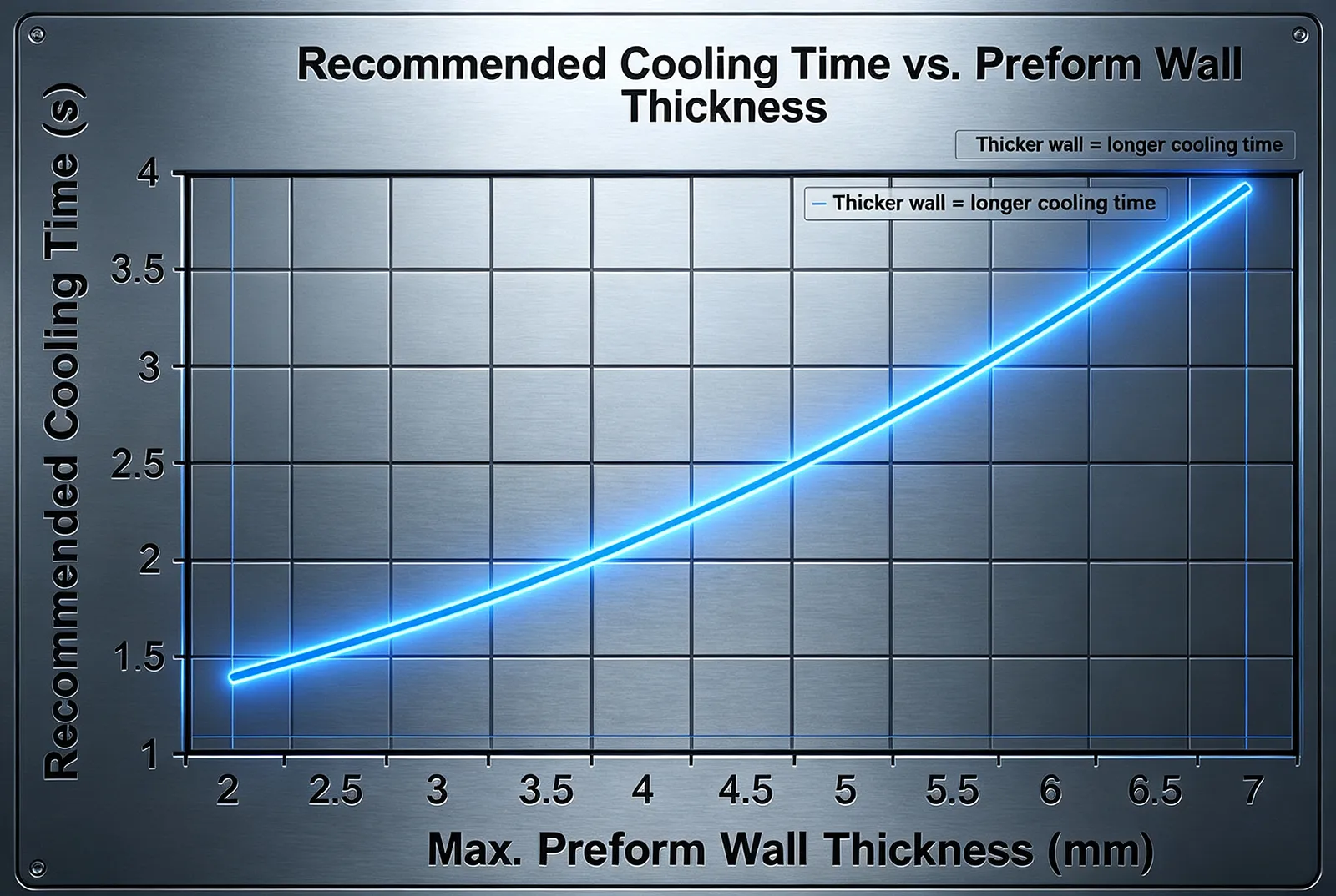
يوضح الرسم البياني أن زيادة سماكة الجدار يمكن أن تؤدي إلى إطالة مدة التبريد. وهذا يؤثر على تكاليف التصنيع الناتجة.
6. فتح القالب وإخراج المنتج
بعد أن يبرد القالب بشكل كافٍ، يقوم المهندسون بفتحه. ويتم إزالة المكون عن طريق إخراجه باستخدام دبابيس الإخراج والأكمام وآليات أخرى. وأثناء عملية الإخراج، يجب توخي أقصى درجات الحذر لتجنب حدوث أي أعطال. ففي حين أن الأجزاء البلاستيكية التقليدية يمكنها تحمل قوى الإخراج المفرطة، فإن مجموعة لوحات الدوائر المطبوعة (PCB) المُقولبة قد لا تتحمل مثل هذه القوى. فقد تنتقل القوة المفرطة إلى المكونات الموجودة على لوحة الدوائر المطبوعة (PCB)، مما يؤدي إلى كسرها. بعد الإخراج، قد يخضع المكون لعمليات معالجة لاحقة وفحص للتأكد من فعالية المنتج وسلامته. يوضح الجدول التالي بعض معايير الاختبار.
| الفحص | ما الذي يكتشفه |
|---|---|
| الفحص البصري | ومضات، لقطات قصيرة، حروق، تشققات |
| فحص الأبعاد | الالتواء والأبعاد الحرجة |
| الأشعة السينية/التصوير المقطعي المحوسب | الفراغات، الإزاحة الداخلية، التغليف |
| الاستمرارية الكهربائية | الدوائر المفتوحة |
| مقاومة العزل | مشاكل العزل الكهربائي |
| اختبار الجهد العالي | الانهيار العازل |
| الاختبار الوظيفي | التشغيل الإلكتروني |
| اختبار التسرب | سلامة الهيكل/السد |
| الدورات الحرارية | الموثوقية الحرارية-الميكانيكية |
| اختبار الشد/التقشير | التصاق السطح عند الاقتضاء |
لماذا لا يمكنك ببساطة استخدام تقنية القولبة بالحقن القياسية لتصنيع لوحة الدوائر الكهربائية؟
على الرغم من أنه من الممكن تغليف بعض لوحات الدوائر المطبوعة باستخدام القولبة بالحقن بالحرارة، إلا أن المهندسين يحتاجون إلى درجة عالية من الحذر، لا سيما في حالة لوحات الدوائر المطبوعة المليئة بالمكونات. فقد تؤدي عملية القولبة بالحقن التقليدية ذات الضغط العالي إلى تعطل المكونات. ومن بين المعلمات التي تعيق تطبيق عملية القولبة بالحقن التقليدية: الضغط، ودرجة الحرارة، والتدفق، والانكماش، والحمل الميكانيكي.
خلال عملية القولبة بالحقن التقليدية، يكون ضغط التجويف الناتج عن البلاستيك المنصهر أعلى نسبيًا من الضغط المنخفض المخصص المستخدم في القولبة فوق لوحات الدوائر المطبوعة (PCB). ويؤدي هذا الضغط المرتفع إلى ممارسة قوة أكبر على مكونات لوحات الدوائر المطبوعة، مثل المكثفات الخزفية، وحزم BGA، والمقاومات SMD، والموصلات، وأجهزة الاستشعار، والأطراف الملحومة، والمكونات ذات المسافات الدقيقة. ويزداد خطر الإزاحة أو الحمل الميكانيكي بشكل أكبر عندما تحتوي اللوحة على مكونات كبيرة الحجم أو غير مدعومة. ووفقًا لشركة Henkel، فإن القولبة بالضغط المنخفض هي عملية خاصة لتغليف المكونات الهشة بأمان. وعادةً ما تتم معالجة المواد المستخدمة في طريقة الضغط المنخفض عند ضغط أقل من تلك المستخدمة في عملية القولبة بالحقن التقليدية.
تعد درجة الحرارة عاملاً آخر يدفع إلى عدم استخدام عملية القولبة بالحقن التقليدية. فالعديد من اللدائن الحرارية الهندسية تتطلب درجات حرارة انصهار عالية نسبيًا حتى تتدفق. من ناحية أخرى، يجب أن يلتزم تجميع لوحات الدوائر المطبوعة (PCB) بالحدود الحرارية المحددة لمكوناته وموصلاته ووصلات اللحام والمواد اللاصقة. وقد يؤدي هذا التناقض إلى تعقيد عملية التصميم من الناحية الفنية.
ما هي أفضل المواد المستخدمة في عملية التشكيل الفوقي للوحات الدوائر المطبوعة (PCB)؟
لا توجد قاعدة عامة لاختيار أفضل المواد المستخدمة في عملية القولبة الفوقية للوحات الدوائر المطبوعة (PCB). فكل مادة تناسب تطبيقات مختلفة. وفي معظم المشاريع، ينبغي أن تتضمن القائمة الأولية للمواد المختارة: مواد البولي أميد القابلة للذوبان بالحرارة تحت ضغط منخفض، والبولي يوريثان، والإيبوكسي، والسيليكون، وبعض أنواع الإيلاستومرات الحرارية، حيث توفر كل منها خصائص حرارية وميكانيكية مميزة لتغليف المكونات الإلكترونية [3].
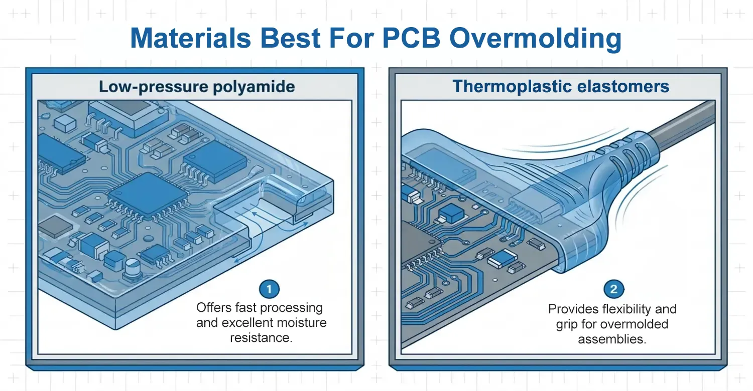
| المواد | الدور النموذجي | المزايا الرئيسية | القيود الرئيسية |
|---|---|---|---|
| البولي أميد منخفض الضغط | القولبة الفوقية للوحات الدوائر المطبوعة (PCB) واللوحات المجمعة (PCBA) | سرعة المعالجة، ومقاومة الرطوبة، ودرجات مرنة | يجب التحقق من نطاق درجات الحرارة وتوافق المواد |
| البولي يوريثان | التغليف/التثبيت | مرونة جيدة وحماية البيئة | تتطلب كيمياء العلاج والخصائص طويلة الأمد عملية التحقق من صحتها |
| إيبوكسي | التغليف الصلب | مقاومة كيميائية وميكانيكية عالية | صلب؛ يصعب إصلاحه؛ يولد المعالجة حرارة |
| سيليكون | التغليف المرن | مرونة ممتازة ومقاومة ممتازة لدرجات الحرارة | قوة ميكانيكية أقل؛ يتعين التحقق من صحة التماسك |
| TPE/TPU | القولبة المرنة | المرونة، والثبات، وتخفيف الضغط | تعتمد الحدود الحرارية والكيميائية بشكل كبير على التركيبة |
| PC/ABS التقليدي | غلاف هيكلي/تشكيل بالقولبة | خصائص ميكانيكية وجمالية جيدة | غالبًا ما تكون غير مناسبة للتغليف المباشر تحت ضغط عالٍ للوحات الدوائر المطبوعة (PCBA) الحساسة |
الخاتمة
يُعد القولبة الفوقية للوحات الدوائر المطبوعة (PCB) أمرًا ضروريًا في العديد من التطبيقات الإلكترونية. وتتمثل هذه العملية في تغطية لوحة الدائرة المطبوعة المُجمَّعة (PCBA) بمادة عازلة، مثل البلاستيك. ويعتمد نوع المادة المستخدمة على مستوى الحماية المطلوب واحتياجات مرونة اللوحة.
المرجع
[1] المنظمة الدولية للتوحيد القياسي (ISO). (2018). ISO 16750-1:2018 المركبات البرية — الظروف البيئية واختبارات المعدات الكهربائية والإلكترونية. منصة التصفح عبر الإنترنت (OBP) التابعة للمنظمة الدولية للمعايير (ISO). https://www.iso.org/obp/ui/#iso:std:iso:16750:-1:ed-3:v1:en
[2] ScienceDirect. (بدون تاريخ). معادلة هاغن-بوازيل – نظرة عامة. موضوعات ScienceDirect. https://www.sciencedirect.com/topics/engineering/hagen-poiseuille-equation
[3] ScienceDirect. (بدون تاريخ). الاستومر الحراري – علم المواد. موضوعات ScienceDirect. https://www.sciencedirect.com/topics/materials-science/thermoplastic-elastomer



 AR
AR  EN
EN  ES
ES  FR
FR  DE
DE  IT
IT  PT
PT  NL
NL  PL
PL  JA
JA  KO
KO  ZH
ZH