

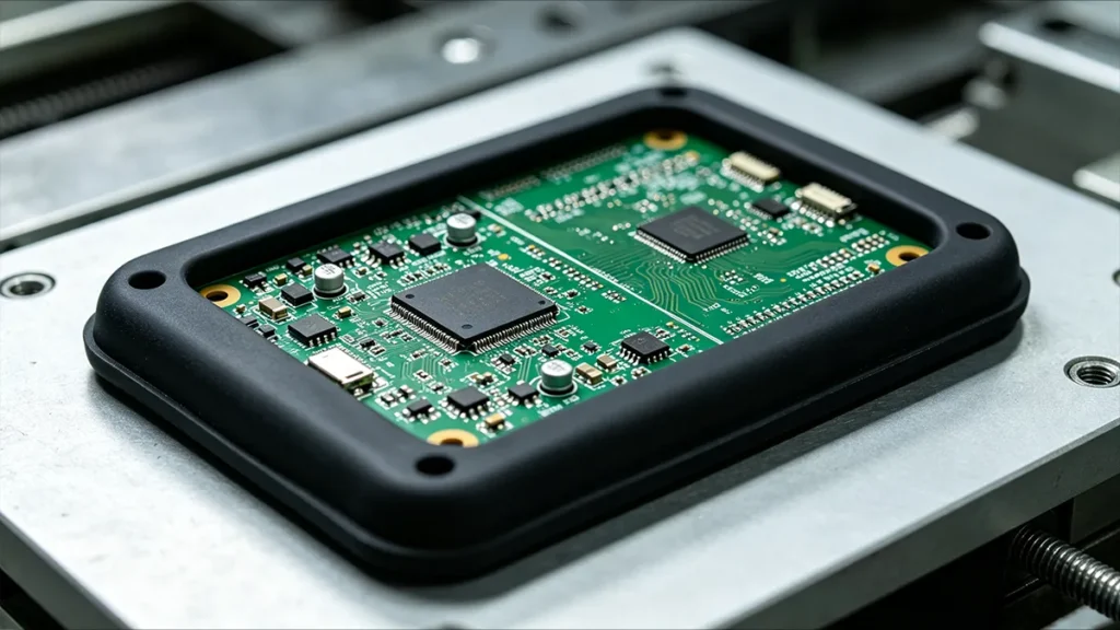
A steering wheel switch assembly may appear to be a simple device, but it is complex in design. The assembly includes LEDs, resistors and capacitors, tactile switches, an FR-4 PCB, an automotive connector, and a Microcontroller. These devices must be well protected during vehicle operations. The vehicle is exposed to a demanding environment characterized by humidity, vibration, temperature cycling, and mechanical loading, which strictly necessitates compliance with environmental reliability standards such as ISO 16750 for automotive electronics [1]. It is essential to select the appropriate manufacturing process to protect these devices in this operational environment. The most preferred manufacturing method is overmolding the printed circuit board (PCB) with thermoplastic elastomer (TPE). The overmolded PCB is electrically insulated and protected against vibration.
What is PCB Overmolding?
PCB overmolding is the process of enveloping an assembled circuit board in rubber or plastic using the injection molding process. The PCB assembly is placed in a custom mold, and molten material is poured into the cavity. The material cools, forming a solid protective shell around the board.
PCB Overmolding Process
PCB overmolding process is almost similar to conventional injection molding. In fact, the process uses equipment similar to that used in conventional injection molding. However, the process window for PCB overmolding is substantially tighter than for ordinary plastics. The following is the sequential flow of the events in the PCB overmolding process:
- PCB inspection
- Cleaning / Drying
- Insert
- Loading & Positioning
- Mold Closing
- Melting
- Injection
- Packing / Holding
- Cooling
- Mold Opening
- Ejection
- Trimming + Inspection
- Electrical / Functional Testing
1. Inspection of the PCB circuit
Before commencing the overmolding process, ensure that all circuits on the circuit board are fully soldered and tested to confirm there are no issues. Once the encapsulation is complete, it is impossible to rework the internal parts. After confirming everything, the next step is to clean the circuit board. Sometimes, a primer layer needs to be applied to the surface to enhance adhesion between the material and the circuit board and to prevent future detachment or water ingress.
2. Mold Design and Fabrication
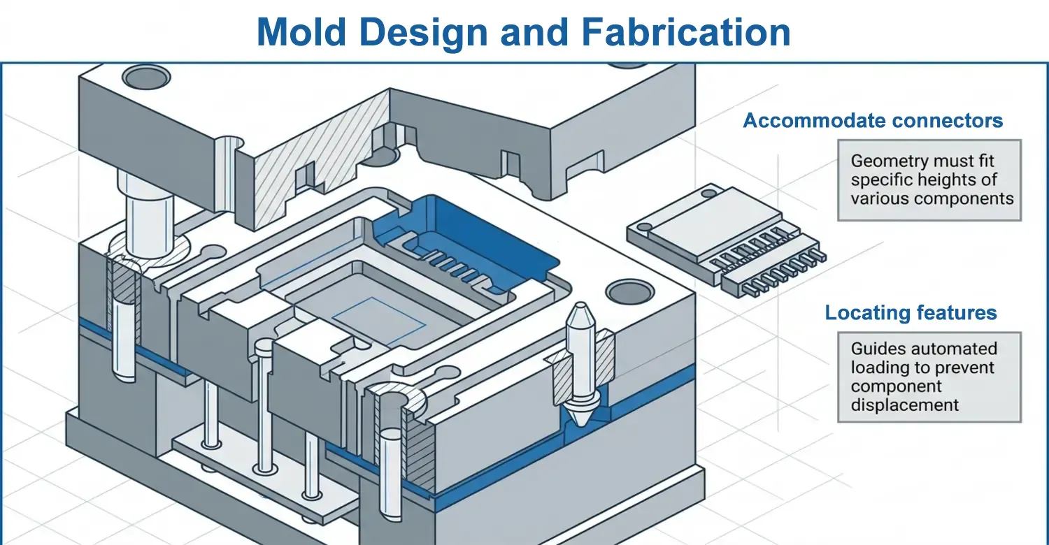
PCB overmolding succeeds well with investment in the mold design. The mold cavity used in PCB overmolding has a geometry that differs from that of ordinary injection molding. The cavity has to accommodate connectors, solder joints, and electronic components. The designer must ensure that the mold is effectively fixed to avoid any movement during injection. A very small displacement is undesired because it can lead to connector misalignment, uneven encapsulation thickness, and component damage. If the mold is intended for high volumes, it is necessary to use locating features to guide the automation of PCB loading.
Effective mold inspection must be conducted before molding. Prior inspection helps to identify possible contamination and solder defects. Once the mold is inspected, it should be cleaned to prevent polymer adhesion and void formation, which affect product quality. Preparation can also involve drying the mold, especially where moisture-sensitive polymers are used. These polymers can absorb water, dissolve, and change their chemical and physical properties when exposed to humid environments. Such moisture-sensitive engineering polymers commonly used in overmolding include Nylons (Polyamides), Polyurethanes (PU), and certain Thermoplastic Elastomers (TPE).
3. Loading and Mold Closure
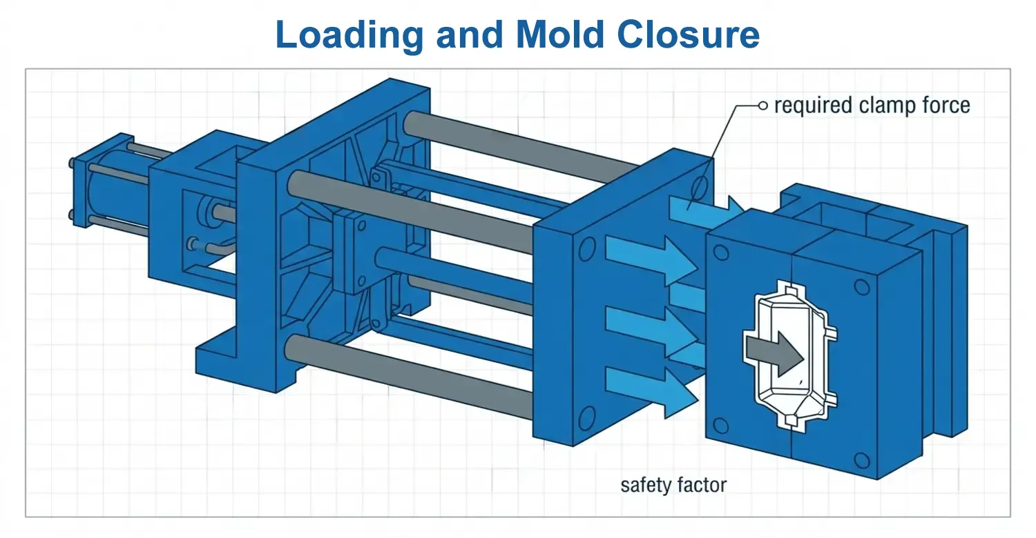
After inspection, the PCBA is placed in the designed mold. The mold will precisely hold its position to ensure that the encapsulated material flows accurately to every area without damaging the components. Once loading is complete, the operator closes the mold around the PCB to begin the injection process. The injection of the molten material into the cavity occurs under pressure, which implies the application of sufficient clamping force. When choosing the clamping force, ensure it is higher than the required clamp force. This relationship is given as;
Fc = PcApS
Where Fc is the required clamp force, Pc is the effective cavity pressure, and Ap is the projected area of the molded component. S is the safety factor. If, for instance;
Pc=60MPa, and Ap= 0.004m2, then
Fc=60×106×0.004=240kN.
When designing the mold, engineers selected a safety factor to ensure the clamping force exceeded the cavity pressure. For instance, choosing a safety factor of 1.5 would adjust the clamping force to 360 kN, which is much safer for injecting molten materials. The clamp force must be selected at a moderate value. Insufficient clamp force can produce parting-line flash, while excessive clamp force can increase tool stress and energy consumption.
4. Plastic Melting and Injection
A long cylindrical barrel with a rotating screw contains heaters that melt plastic resin. The screw mixes and builds pressure for the resin, pushing it forward. The molten plastic is injected into the cavity under controlled pressure. The pressure varies due to different factors like velocity, wall thickness, polymer viscosity, and gate design, as summarized in Newtonian flow through a circular channel given by;
ΔP≈8μLQ/πR4 [2]
Where ΔP is pressure drop, μ is melt viscosity, L is flow length, Q is volumetric flow rate, and R is effective flow radius. While most plastics don’t follow this Newtonian flow equation, it guides engineers in identifying critical areas to observe when exerting or regulating injection pressure.
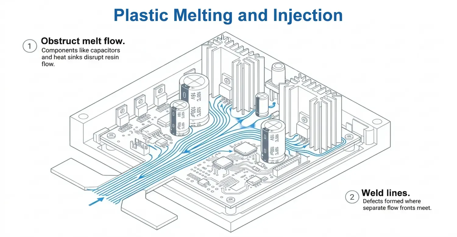
The flow of materials in the mold cavity for PCB overmolding is more complex than in conventional injection molding. The PCB assembly contains PCB edges, capacitors, solder joints, IC packages, connectors, wires, heat sinks, and other tall components. These materials can obstruct melt flow. If the obstruction is not well managed, it can result in weld lines that compromise product quality.
5. Cooling and Solidification
Once the cavity is filled, heat must be removed from the polymer. The rate of heat removal is directly proportional to the wall thickness.
tc ∝ s2
where tc is the cooling time, and s is the characteristic polymer thickness.
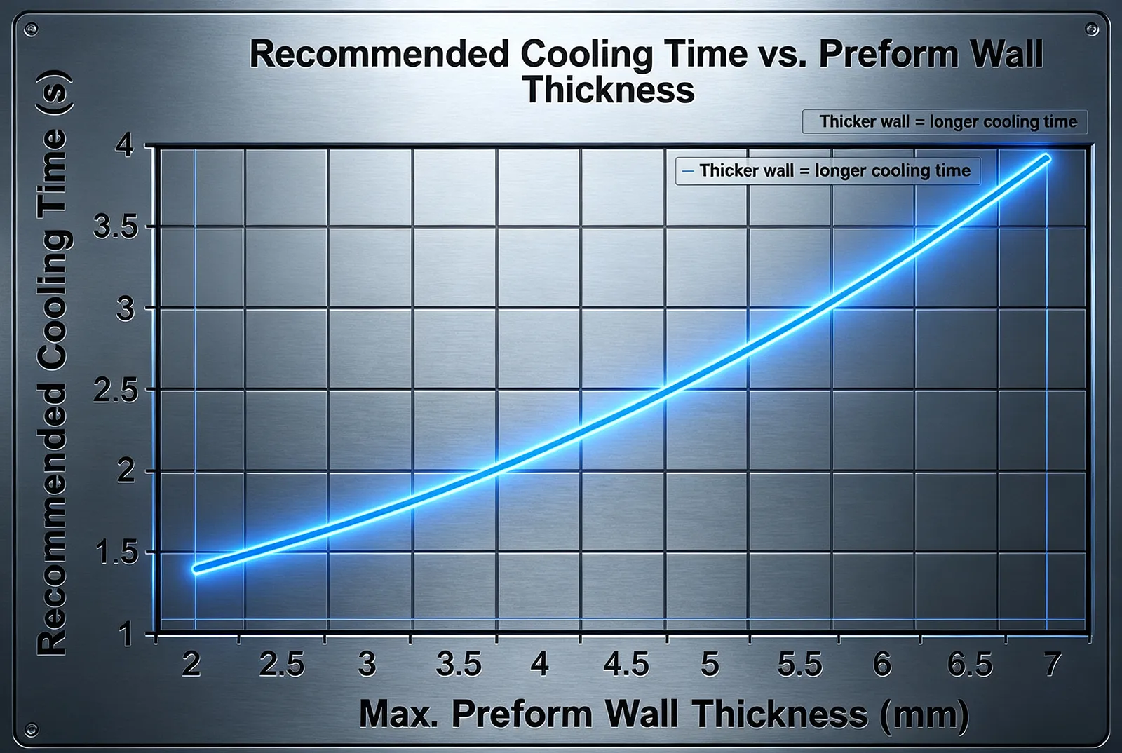
The graph shows that increasing wall thickness can lengthen the cooling time. This affects the resulting manufacturing costs.
6. Mold Opening and Ejection
After the mold has sufficiently cooled, engineers open it. The component is removed by ejecting it using ejector pins, sleeves, and other mechanisms. During ejection, most care should be observed to avoid failures. While conventional plastic parts can withstand excessive ejection forces, an overmolded PCB assembly may not withstand such forces. Excessive force can be transferred to components on the PCB, leading to breakage. After ejection, the component may undergo post-processing and inspection to ensure that the product is effective and safe. The following table highlights some of the test criteria.
| Inspection | What it detects |
|---|---|
| Visual inspection | Flash, short shots, burns, cracks |
| Dimensional inspection | Warpage and critical dimensions |
| X‑ray/CT | Voids, internal displacement, encapsulation |
| Electrical continuity | Open circuits |
| Insulation resistance | Electrical isolation problems |
| Hi‑pot testing | Dielectric breakdown |
| Functional testing | Electronic operation |
| Leak testing | Housing/sealing integrity |
| Thermal cycling | Thermo‑mechanical reliability |
| Pull/peel testing | Interface adhesion where applicable |
Why Can’t You Simply Use Standard Injection Molding For A Circuit Board?
Even though it is possible to encapsulate some circuit boards using thermoplastic injection molding, engineers require a high level of care, especially for populated PCBs. Conventional high-pressure injection molding can lead to component failure. Some of the parameters hindering the application of the conventional injection molding process include pressure, temperature, flow, shrinkage, and mechanical loading.
During conventional injection molding, the cavity pressure generated by molten plastic is relatively higher than the specialized low pressure used in PCB overmolding. This high pressure exerts greater force on PCB components such as ceramic capacitors, BGA packages, SMD resistors, connectors, sensors, soldered terminals, and fine-pitch components. The risk of displacement or mechanical loading is even higher when the board contains large or unsupported components. According to Henkel, low-pressure molding is a special process of safely encapsulating fragile components. The materials used in the low-pressure method are usually processed at lower pressure than those in the conventional injection molding process.
Temperature is another consideration for not using the conventional injection molding process. Many engineering thermoplastics require relatively high melt temperatures to flow. On the other side, PCB assembly must maintain thermal limits for its components, connectors, solder joints, and adhesives. This contradiction can technically complicate the design process.
What Materials Are Best For PCB Overmolding?
There is no rule of thumb on selecting the best materials for PCB overmolding. Different materials suit different applications. In most projects, the initial material shortlist should include low-pressure polyamide hot melts, polyurethane, epoxy, silicone, and selected thermoplastic elastomers, each offering distinct thermomechanical properties for electronic packaging [3].
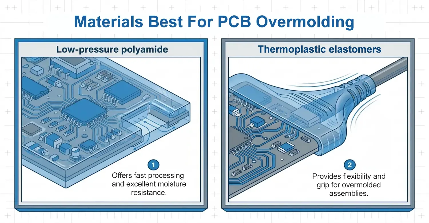
| Material | Typical role | Main advantages | Main limitations |
|---|---|---|---|
| Low‑pressure polyamide | PCB/PCBA overmolding | Fast processing, moisture resistance, flexible grades | Temperature window and material compatibility must be verified |
| Polyurethane | Encapsulation/potting | Good flexibility and environmental protection | Cure chemistry and long‑term properties require validation |
| Epoxy | Rigid encapsulation | High chemical and mechanical resistance | Rigid; repair is difficult; cure generates heat |
| Silicone | Flexible encapsulation | Excellent flexibility and temperature resistance | Lower mechanical strength; adhesion requires validation |
| TPE/TPU | Flexible overmolding | Elasticity, grip, strain relief | Thermal and chemical limits depend strongly on formulation |
| Conventional PC/ABS | Structural enclosure/overmold | Good mechanical and cosmetic properties | Often unsuitable for direct high‑pressure encapsulation of delicate PCBAs |
Conclusion
PCB overmolding is essential in many electronic applications. It involves covering a PCBA with an insulating material, such as plastic. The type of material to use depends on the desired protection level and board flexibility needs.
Reference
[1] International Organization for Standardization (ISO). (2018). ISO 16750-1:2018 Road vehicles — Environmental conditions and testing for electrical and electronic equipment. ISO Online Browsing Platform (OBP). https://www.iso.org/obp/ui/#iso:std:iso:16750:-1:ed-3:v1:en
[2] ScienceDirect. (n.d.). Hagen-Poiseuille Equation – an overview. ScienceDirect Topics. https://www.sciencedirect.com/topics/engineering/hagen-poiseuille-equation
[3] ScienceDirect. (n.d.). Thermoplastic Elastomer – Materials Science. ScienceDirect Topics. https://www.sciencedirect.com/topics/materials-science/thermoplastic-elastomer





 EN
EN  ES
ES  FR
FR  DE
DE  IT
IT  PT
PT  NL
NL  PL
PL  AR
AR  JA
JA  KO
KO  ZH
ZH