The performance of PVD coatings is a function not only of equipment and processes but also of the quality and characteristics of input materials. While PVD process engineers may focus on variables like base pressure, plasma formation, substrate bias, etc., the final coating also depends on the quality of all source inputs. No matter how clean your system is or how perfect your gas flow rates are, inferior materials will degrade performance.
For OEMs, engineers, or materials buyers, the sourcing of PVD targets is a highly strategic step that must consider coating repeatability, applicability of the material to the coatings being applied, and long-term process reliability. This guide seeks to frame things in a way to help understand compatibility of material structures, deposition methods, and supplier capabilities to ensure consistent process windows free of defects.

What PVD Target Materials Need to Satisfy for Different Thin Film Applications
Material selection for thin film coatings under PVD should start with the requirements of the application, the substrates being coated, and the target coatings, rather than from price or other factors. Different PVD coating applications have drastically different requirements:
- Optical Coatings: Require specific refractive indices to modify light reflection and transmission.
- Aesthetic Coatings: Often rely on carefully controlled plasma conditions to achieve the desired color, while also being selected for surface durability and scratch resistance.
- Electronics: Often require tightly controlled electrical properties, film purity, and conductivity depending on the device architecture.
The PVD target materials you buy should be selected around those requirements, whether the priority is corrosion resistance, wear resistance, low friction, or another performance target.
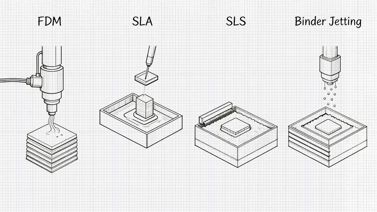
Sputtering Target Materials Versus Evaporation Materials for PVD – Which One Works with Your System?
Before you start considering chemistry, you should validate process compatibility. There are two major types of physical deposition, and each requires entirely different materials based on their vaporization routes:
Sputtering Targets
The advantages of sputtering are that the solid phase is converted to vapor not by heating it, but rather via energetic plasma bombardment that physically displaces surface atoms. This works well for complex materials or those with high melting points. Sputtering is often selected when dense films, good uniformity, and strong adhesion are important, such as in optical or semiconductor applications.
Evaporation Materials
Thermal evaporation or e-beam is what it sounds like, and allows simple metallization layers to be evaporated, or higher throughput layers. These coatings have a higher rate of deposition, but lower energy and moderate density compared to sputtered films.
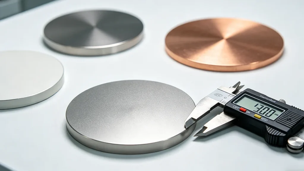
How Purity, Density, and Crystalline Structure Impact Coating Outcomes
There are technical traits in source materials that place a hard ceiling on how well the coating behaves downstream. To be repeatable in production, you must understand four fundamental raw material properties:
Purity: Purity sets up the baseline for operation, and poor quality ends up making coatings more defective. Contaminants tend to be points of physical failure in the coating underneath during the PVD process. For example, unwanted impurities in metallic targets can affect film adhesion, electrical performance, or downstream device reliability. Metal contaminants will alter the resistance of coatings. In semiconductor-grade materials, impurity control must be extremely tight, as trace contaminants can affect device performance and long-term reliability.
Gęstość: Density governs the stability of the deposition process. Targets often have a density of ≥98% theoretical density. Low-density porous materials entrap gases, causing them to outgas during deposition, which causes problems like arcing (electrical discharges that shoot macro particles onto the surface, causing defects).
Grain Structure: Grain size and orientation on the target surface affect erosion uniformity. Grain size and grain uniformity can influence erosion behavior and sputtering consistency, while coarse or uneven microstructures may contribute to less uniform target wear.
Repeatability: Targets that experience density variation and have non-consistent grain populations will sputter unevenly, causing unpredictable variations in coating thickness that harm yield in repeated runs.
Why PVD Coating Materials Aren’t Interchangeable
Mistreating input materials as generic will cause coating failure modes to proliferate inefficiently. Different coating environments require different chemical spaces and it’s critical to recognize this as a decision point.
Coating System Materials and Wear Coatings: Tribological environments often require coatings that reduce friction and improve surface durability. Coatings such as ta-C (tetrahedral amorphous carbon) are valued for their very high hardness, low friction, and strong wear resistance in demanding applications.
Electronics and Conductive Environments: Conductive layouts require a variety of tradeoffs—Al is nearly universally used for interconnects due to thermal stability and low cost, but Au is necessary when wire bonding materials that require oxidation resistance, and Cr is selected when hardness and corrosion resistance are more critical than conductivity.
Optical Coatings: Uses of transmissive and reflective coatings requires exploitation of thin film interference in lenses to reduce light reflection, requiring highly transparent dielectrics and oxide materials (TiO2, ZnO, etc.) with specific refractive indices. Coating thickness of these evaporated elements is controlled to manipulate the reflection and transmission of light.
Energy Coatings and Other Specialty Industrial Coatings: Solar coatings often require a combination of transparency, conductivity, and application-specific efficiency targets. Materials such as ITO are widely used in transparent conductive layers, while systems such as CIGS continue to be used in high-performance thin-film solar applications. As with other coating categories, real-world operating requirements should drive target material selection.
What to Look for in a Thin Film Materials Vendor
Once the correct chemical composition has been identified, potential vendors should be evaluated on more than just the material name and price. You need to ensure that your vendor has strong QA systems and supporting documentation, and when working with bonded assemblies, that appropriate inspection and testing are used to verify bond integrity.
You also need to understand their custom capability and product portfolio—do they offer optimized grain size? Crystallographic orientations? Custom sizes? Turnaround time? And technical support? A lot of this is needed to ensure continuous production and reliability. Even when the correct category of material is selected, you’ll find that results depend on working with a supplier of high-quality thin film materials that is able to offer consistent specs, customized needs, and helps connect the dots with PVD process requirements.
Mistakes Made When Selecting PVD Materials
Sourcing the wrong input materials can bottleneck your PVD process. Here are 5 major mistakes that should be avoided:
- Sourcing by price only and ignoring density flaws. Lower-cost materials may not always meet the density and structural consistency needed for stable sputtering, which can lead to faster target wear and less reliable production.
- Ignoring purity requirements. Failing to exclude elements in parts per billion analytic levels can ruin optical coating systems with unwanted impurities like Fe that otherwise cause failure modes.
- Failing to check deposition-method compatibility. Material properties need to be matched to the equipment being used. For example, ceramic and insulating materials often require different sputtering configurations than conductive metals, and thermal behavior should be considered when selecting both the target and the process.
- Failing to consider application specific performance needs. Using default geometries for ferromagnetic materials like Fe or Ni instead of custom sized shapes which disrupt the magnetic flux needed to sustain plasma in specialized tools.
- Failing to QC suppliers before ordering. Minor steps avoided create major mechanical failure risks from atomic diffusion in bonding layers, etc.
Closing Thoughts on PVD Coating Materials
It’s important to remember that PVD coating success requires the right materials to be selected to match both the structural application and physics deposition process. Defect-free operation depends on balancing material requirements with process needs and working with a vetted vendor that can support consistent downstream performance.